
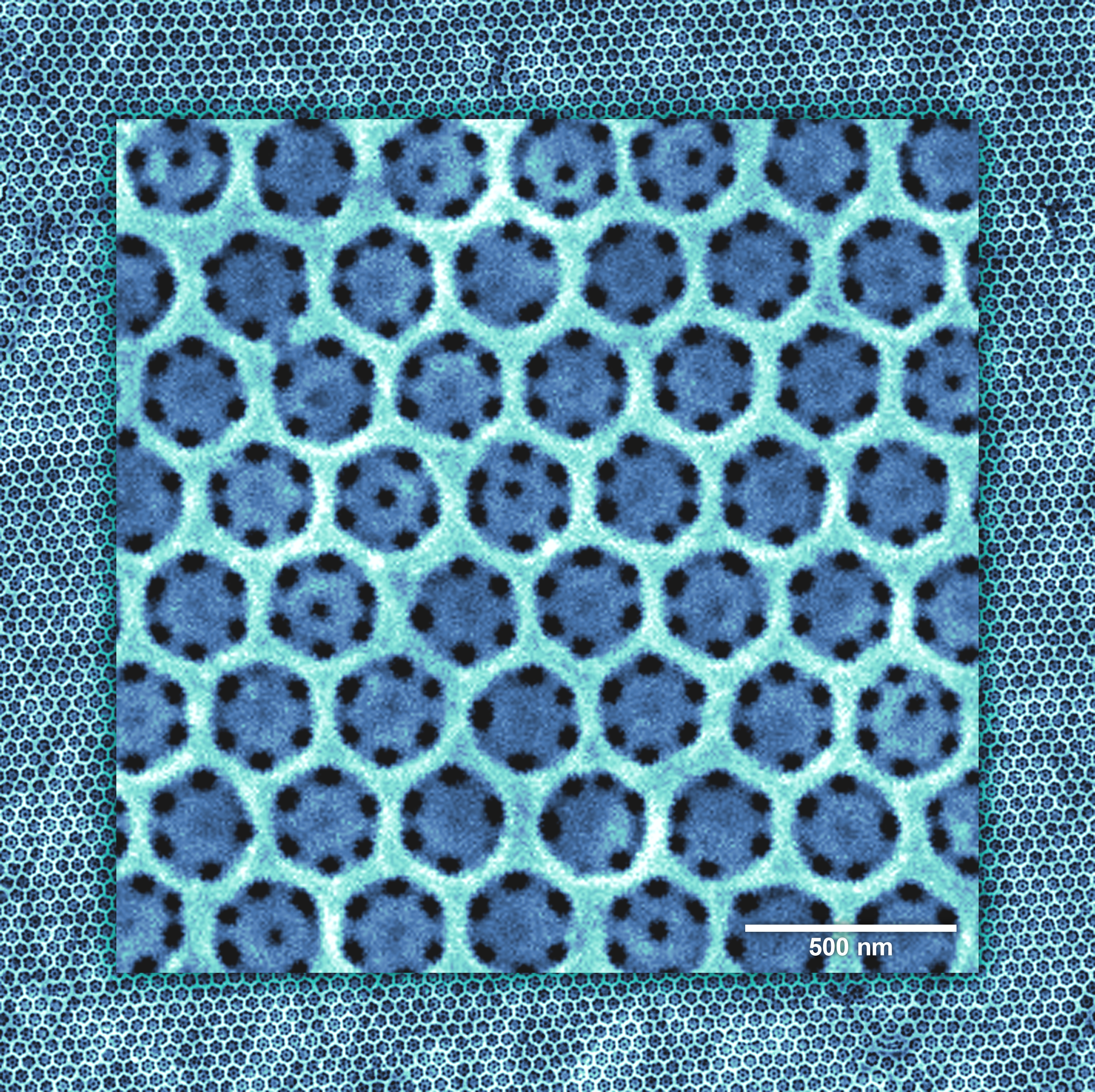
image: Dense and large-scale homogeneous coating of metal surfaces with titanium oxide nanostructures, created at the Institute of Nuclear Physics of the Polish Academy of Sciences. Artificial colors.
Credit: Source: IFJ PAN
Cracow, 7 August 2025
Nanostructures transcend boundaries (of grains in metals)
Large metal surfaces coated with precisely formed nanostructures have so far remained in the realm of fantasy. The obstacle standing in the way of their production seemed fundamental, as it resulted from the presence of crystal grains in metals: their boundaries disrupted the growth of the nanostructures. At the Institute of Nuclear Physics of the PAS, using titanium and its oxide by way of example, it has been proven that this obstacle can be overcome.
Coatings made of nanostructures with precisely selected sizes and shapes make it possible to control material properties. Unfortunately, in the case of most metals, there was a serious limitation: it was impossible to produce homogeneous coatings on large surfaces due to the disturbances appearing at the boundaries of the crystal grains. This limitation has been overcome at the Institute of Nuclear Physics of the Polish Academy of Sciences (IFJ PAN) in Cracow, where the process of large-area metal coating with nanotubes has been demonstrated using titanium and its oxide as an illustration. This achievement seems promising in the context of many applications, among which medical implants, photovoltaic cells, chemical detectors, and memristors stand out.
“We are unique in the world in our ability to coat large areas of titanium sheet metal, measuring tens of square centimetres, with titanium oxide nanotubes in a strictly controlled manner. The method we propose is the result of combining two unconventional techniques for nanostructuring material surfaces: nanoparticle lithography and electrochemical anodization,” says Dr. Eng. Juliusz Chojenka (IFJ PAN), the first author of the article describing the achievement, published in Acta Materialia.
Both nanoparticle lithography and anodization are techniques that have been known for a long time, but they have only been used on a laboratory scale and have not hitherto been combined. The physicists from Cracow emphasise that the advantage of their proposed method is its simplicity, speed, low production costs, and the possibility of easily scaling the entire process in a way that allows for technological applications, such as the production of large-area coatings.
Nanoparticle lithography plays a role in the first, preparatory phase of manufacturing titanium oxide nanotube coatings. The main protagonists here are spherical polystyrene nanoparticles, commercially available in diameters ranging from 50 nanometres to several dozen micrometres. Nanospheres of a selected diameter are introduced into water in such quantities that, when they float to the surface, they form a single layer of the desired size. Because the nanoparticles are electrically charged during this process, they push each other apart, resulting in their even distribution, characterised by hexagonal regularity.
The highly uniform monolayer of polystyrene nanoparticles is then deposited on a polished titanium plate. The nanoparticle-coated material is now placed in a vacuum chamber, where it is exposed to plasma generated from nitrogen and oxygen for several minutes. Under its influence, the polystyrene spheres shrink slightly, but retain their original positions. The sample is then transferred to another vacuum chamber, where a thin layer of titanium is deposited on it. The final stage of the lithographic phase is the removal of the nanoparticles using an organic solvent and ultrasound, which causes the sample to vibrate. The result is a surface covered with a hexagonal, regular grid of pits called antidots.
“In a special chamber, we now subject the sample covered with antidots to anodization, i.e. an electrochemical process resulting in the formation of uniform and ordered nanostructures on its surface,” explains Dr. Eng. Michal Krupinski (IFJ PAN) and adds: “By skilfully selecting the composition of the electrolyte in which anodization takes place, and by controlling the applied voltage, temperature and time, we are able to form a dense coating of titanium oxide nanotubes, arranged in accordance with the original antidot pattern and with a predetermined length, which in the case described in our article is 15 micrometres.”
It should be emphasised here that standard titanium anodization is subject to severe physical limitations regarding the scale of orderliness of the nanostructures, resulting from the size of the crystal grains in the metal matrix. This is why the physicists in Cracow precede anodization with a nanopatterning process using nanoparticle lithography. Lithography allows for the modification of the electric field distribution on the titanium surface, which is important during anodization, thereby forcing the long-range ordering of the nanostructures that are formed.
The physical and chemical properties of the coatings obtained in this way were comprehensively characterised using scanning electron microscopy, X-ray diffraction, and Raman spectroscopy, and their photoactivity under ultraviolet radiation was also determined. During several days of testing, it was found that despite exceeding the boundaries of the crystal grains, the nanotube coatings produced are mechanically durable, and the nanotubes themselves do not break even during annealing.
The presented method of titanium oxide nanostructuring has the potential for wide application. Medical implants could be coated with nanotubes that release drugs into the body in a controlled manner, improving biocompatibility. By skilfully selecting the size and density of the nanotubes, it is possible to control the photoactivity of titanium oxide interacting with ultraviolet radiation, which encourages applications related to photovoltaic cells or the control of chemical reactions. It is also known that the surface of titanium oxide changes its properties depending on the adsorption of even small amounts of hydrogen, so new, more sensitive detectors than those currently available are also being considered. Interesting prospects are emerging in the miniaturisation of memristors, i.e., electronic components whose resistance depends on the history of the current flowing through them. Currently, memristors, which are promising components of new types of memory and artificial synapses, are tens of micrometres in size. Meanwhile, their function could be taken over by single nanotubes – objects at least a hundred times smaller.
“There are no physical, chemical, or technical obstacles to adapting our method to the nanostructuring of surfaces made of transition metals other than titanium, such as iron, aluminium, or tantalum. It all depends on the needs,” Dr. Chojenka concludes.
Research conducted by materials physicists from the Institute of Physics of the Polish Academy of Sciences was funded by a grant from the Polish National Science Centre. The chemical analysis was carried out in collaboration with the Faculty of Chemistry at Jagiellonian University.
The Henryk Niewodniczański Institute of Nuclear Physics (IFJ PAN) is currently one of the largest research institutes of the Polish Academy of Sciences. A wide range of research carried out at IFJ PAN covers basic and applied studies, from particle physics and astrophysics, through hadron physics, high-, medium-, and low-energy nuclear physics, condensed matter physics (including materials engineering), to various applications of nuclear physics in interdisciplinary research, covering medical physics, dosimetry, radiation and environmental biology, environmental protection, and other related disciplines. The average yearly publication output of IFJ PAN includes over 600 scientific papers in high-impact international journals. Each year the Institute hosts about 20 international and national scientific conferences. One of the most important establishments of the Institute is the Bronowice Cyclotron Centre (CCB), which is an infrastructure unique in Central Europe, serving as a clinical and research centre in the field of medical and nuclear physics. In addition, IFJ PAN runs four accredited research and measurement laboratories. IFJ PAN is a member of the Marian Smoluchowski Kraków Research Consortium: “Matter-Energy-Future”, which in 2012-2017 enjoyed the status of the Leading National Research Centre (KNOW) in physics. In 2017, the European Commission granted the Institute the HR Excellence in Research award. As a result of the categorization of the Ministry of Education and Science, the Institute has been classified into the A+ category (the highest scientific category in Poland) in the field of physical sciences.
CONTACTS:
Dr. Eng. Michał Krupiński
Institute of Nuclear Physics, Polish Academy of Science
tel.: +48 12 6628244
email: michal.krupinski@ifj.edu.pl
Dr. Eng. Juliusz Chojenka
Institute of Nuclear Physics, Polish Academy of Science
tel.: +48 12 6628232
email: juliusz.chojenka@ifj.edu.pl
SCIENTIFIC PUBLICATIONS:
“Controlling the Photoactivity of the Nanopatterned Titanium Oxide”
J. C. Chojenka, K. Mróz, A. Bartkowiak, M. Mitura-Nowak, M. S. Shakeri, M. Krupiński
Acta Materialia 2025, 296, 121236
DOI: 10.1016/j.actamat.2025.121236
LINKS:
The website of the Institute of Nuclear Physics, Polish Academy of Sciences.
Press releases of the Institute of Nuclear Physics, Polish Academy of Sciences.
IMAGES:
IFJ250807b_fot01s.jpg
HR: http://press.ifj.edu.pl/news/2025/08/07/IFJ250807b_fot01.jpg
Dense and large-scale homogeneous coating of metal surfaces with titanium oxide nanostructures, created at the Institute of Nuclear Physics of the Polish Academy of Sciences. Artificial colors. (Source: IFJ PAN)
Journal
Acta Materialia
Article Title
Controlling the Photoactivity of the Nanopatterned Titanium Oxide
Article Publication Date
7-Jul-2025